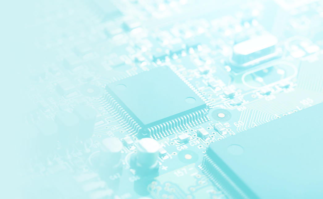
Printed circuit boards (PCBs) are the basic building blocks of today’s electronic devices.
They enable miniaturization and mass machine production of electronic devices: and we are happy to design PCBs exactly for your device.
Support and interest section
Legal informations
They enable miniaturization and mass machine production of electronic devices: and we are happy to design PCBs exactly for your device.
PCB design is one part of the whole process of custom electronics development, the core business of our company. We also offer PCB design as a separate activity – and we can also assemble, revive or certify the designed PCBs.

There is no PCB like a PCB!
PCB design requires a lot of experience: the difference between professional and amateur design often only becomes apparent in mass production.
We care about quality: every design goes through a design review, our checklist has over 60 items. We simulate complex designs first.
FAQ
Are you interested in developing or manufacturing electronics for your company?
Yes – this is a very common model of cooperation. We will take a professional look at the existing PCB and find a way to improve or complete it. Often we don’t even need any documentation.
Design for Manufacturability is the process of optimizing the design of components so that they can be easily and efficiently manufactured. The goal of DFM is to minimize the number of errors in production, increase quality and reliability, reduce costs and shorten production time. That is, to make life easier for production not only with a technically functional design, but with a well thought-out design that is easy to produce.
Because we have our own production, it’s easy to get feedback on the technologies – what solder well, where the scrap is, what confuses the technicians in production. Thanks to this, we are able to design and bring high-end electronics to mass production.
As a rule, the same as elements for series production: mostly in SMT assembly, ready for machine assembly and, if we produce samples in our company, also machine assembled. This facilitates the transition to serial production, we verify the applicability of serial technology during prototyping – it makes little sense to bastlit under a magnifying glass.
The first prototypes and samples usually do not have the tester connections sorted out, and for miniaturized applications we produce larger versions of the boards for hardware debugging.
Electromagnetic compatibility (EMC) is the property of an electrical device that it does not affect other objects, including itself, and that it resists the effects of other devices: it does not interfere with its surroundings (for example, a radio receiver or medical equipment) and is resistant to interference from its surroundings (for example, a mobile phone, large machinery or nearby radar).
The PCB can influence EMC by its design and use in the final application. Some factors that may affect the EMC of a printed circuit board are:
Poorly designed PCBs are a frequent cause of equipment unreliability – especially irregular outages and “hiccups” caused by external interference. Redesigning the PCB often almost miraculously eliminates these problems.
We can design and verify the PCBs correctly according to EMC principles.
Altium Designer
We use professional tools for design: we draw in Altium Designer, one of the most advanced software packages for embedded development. Importantly for our customers and designers, it also generates accurate 3D models of the electronics being developed. Cisco and SpaceX, for example, also work in Altiu.
If necessary, we can process the design in another program (we often use Cadsoft/Autodesk Eagle, OrCAD, Formica or KiCad for some customers).
Contact
Do you need modern and reliable electronics? For integration into your facility or a complete new product or system? Let us know! We are happy to help you with small and complex applications.